Key Takeaways
- PCB manufacturing involves a multi-step process, including design, printing, etching, drilling, plating, and finishing, to create reliable, high-performance circuit boards for electronic devices.
- Quality control measures such as automated optical inspection (AOI), flying probe tests, and X-ray examination ensure each PCB meets strict IPC-A-600 and ISO9001 standards for accuracy and safety.
- Surface finishing options like HASL, ENIG, and OSP protect copper traces from oxidation and improve solderability, supporting various assembly and industry requirements.
- Environmental and worker safety are prioritized throughout production, with strict handling of chemicals, waste management, and compliance with international regulations.
- Common defects like solder bridging, lifted pads, or via issues are minimized through robust design practices, precise manufacturing controls, and consistent quality assurance protocols.
PCB Manufacturing Process
Printed circuit boards (PCBs) are the backbone of nearly all electronic devices we use daily. From mobile phones to kitchen appliances, these small green boards allow complex circuits to function by connecting different components through precise copper pathways.
The manufacturing of PCBs combines cutting-edge technology with detailed craftsmanship. Each production stage must meet strict quality controls to ensure your devices work properly and last a long time. Finding a reliable PCB Manufacturer is essential for creating high-performance electronic products that meet industry standards.
Understanding PCB Manufacturing Basics
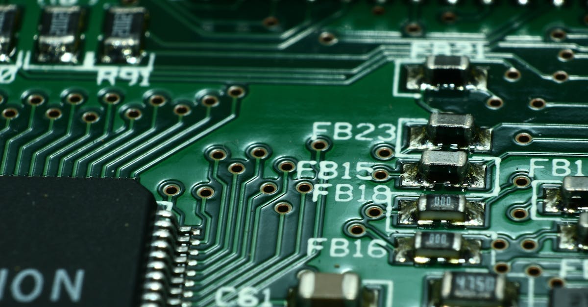
PCB manufacturing combines multiple steps that shape copper-clad laminates into platforms for electronic circuits. The process begins with substrate selection—most commonly fiberglass epoxy (FR4) for durability and performance—before layering copper sheets, which form circuit traces using photolithography and etching. WellPCB in China produces single-sided, double-sided, and multilayer PCBs, using automated processes for mass production and prototype services worldwide.
Designers submit Gerber files, which mapping PCB layouts in digital format. Imaging equipment applies photosensitive film to the copper surface, exposing circuit patterns through ultraviolet light. Chemical baths remove unneeded copper, leaving precise conductive pathways. Engineers verify circuit accuracy by electrical testing after etching and before solder mask application.
Solder mask and silkscreen printing follow, with solder mask covering circuits to protect from oxidation and prevent solder bridges during assembly. Silkscreen ink labels component locations exactly as specified by design files. WellPCB applies surface finishes, including HASL, ENIG, and OSP, to suit RoHS compliance and assembly method requirements.
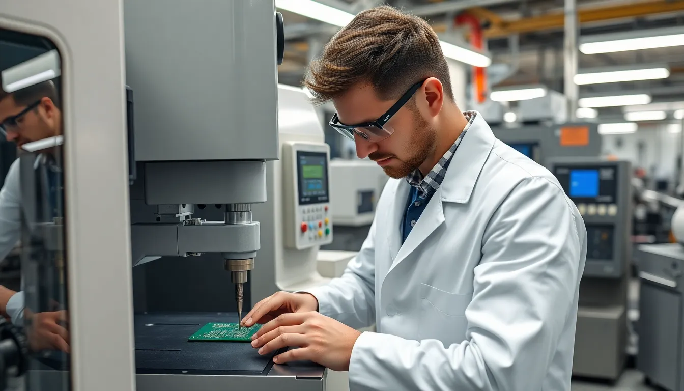
Quality control includes ICT (in-circuit testing), AOI (automated optical inspection), and flying probe tests, ensuring dimensional accuracy and functionality for each batch. WellPCB’s manufacturing standards align with IPC-A-600 and ISO9001 certifications to meet global project and end-product needs.
Key Steps in PCB Manufacturing
PCB manufacturing follows a controlled sequence, converting digital layouts to physical boards. Each step is critical for electrical reliability and precise assembly.
Designing the PCB Layout
PCB layout design defines the board’s electrical functionality and manufacturability. Designers use CAD tools to create files like Gerber or ODB++ that specify copper traces, drill holes, and bill of materials. A design for manufacturability (DFM) check identifies rule violations before production. WellPCB reviews submitted designs to ensure compatibility with automated manufacturing lines and IPC-A-600 standards.
Printing the PCB Design
Printing the PCB design transfers the digital pattern to production films through precision plotter printers. Each PCB layer receives a dedicated film: inner copper, solder mask, and silkscreen. Black and clear inks denote conductive and non-conductive areas on these films. Registration holes set precise layer alignment. WellPCB uses high-resolution imaging to capture intricate circuit details, minimizing registration error during mass fabrication.
Etching the Board
Etching the PCB board removes excess copper from the laminate to expose the designed circuit paths. The copper-clad substrate, usually FR4 epoxy fiberglass, is masked using printed films, then subjected to chemical etchants. This process keeps only the desired copper traces. WellPCB controls etch rates and solution purity to achieve consistent trace widths and to comply with RoHS environmental guidelines.
Drilling and Plating
Drilling and plating establish electrical pathways through the board. Precision CNC machines create vias and through-holes based on drill data. A copper plating process then coats hole walls, connecting circuitry across layers. WellPCB employs automated drilling with tolerance control down to 0.05 mm, ensuring multilayer reliability and improved signal integrity for high-density interconnect (HDI) designs.
Applying Solder Mask and Silkscreen
Applying solder mask and silkscreen protects circuitry and guides component placement. A solder-resistant polymer layer covers exposed copper, except for pads and vias. The silkscreen layer adds component identifiers and assembly markings. WellPCB applies green or custom-color masks and high-contrast silk print, reducing soldering errors and improving trace lifespan during assembly.
Surface Finishing
Surface finishing increases PCB durability and solderability. Surface treatments like HASL, ENIG, or OSP protect exposed copper from oxidation and prepare pads for soldering. WellPCB offers finishes selected to match assembly needs such as high reliability, lead-free standards, or fine-pitch compatibility. Each finish meets IPC and RoHS specifications for global electronics production.
Quality Control and Testing
Manufacturers check each printed circuit board for defects and reliability before shipment. Quality assurance uses automated and manual techniques to meet standards like IPC-A-600 and ISO9001, both followed by WellPCB in China.
Inspection Methods
Automated optical inspection (AOI), X-ray examination, and flying probe testing check PCB integrity. AOI scans copper traces for width, spacing, and solder resist alignment across every panel. X-ray systems view inner layers and solder joints, exposing hidden voids in multilayer boards. Flying probe testers measure resistance and connectivity on production and prototype batches when test fixtures are impractical. WellPCB runs all boards through AOI and electrical testing as part of standard operations.
| Inspection Method | Key Purpose | Common Application Example |
|---|---|---|
| AOI | Visual defect inspection | Soldering accuracy |
| X-Ray | Hidden structure validation | Multilayer trace analysis |
| Flying Probe | Electrical performance check | Prototype test verification |
Common Defects and Solutions
PCBs may show solder bridging, lifted pads, or via/hole integrity issues if production controls lapse. Solder bridging links unintended points after reflow, causing short circuits. Lifted pads break electrical paths due to excessive heat or weak adhesion. Via defects appear from drilling errors or plating inconsistencies. WellPCB minimizes these outcomes by applying improved design-for-manufacturability checks, consistently maintaining equipment, and using high-quality FR4 base materials and copper foils. Operators document defect rates and apply corrective measures when they exceed thresholds, ensuring compliance with both IPC and RoHS criteria for international delivery.
Environmental and Safety Considerations
PCB manufacturing involves chemicals such as photoresist and etching agents, including ammonium persulfate and ferric chloride, each requiring strict handling procedures to protect workers and the environment. WellPCB uses industry-compliant storage and ventilation systems for chemical safety at its China-based facilities. Facility managers require workers to use personal protective equipment—like gloves, goggles, and respirators—during printing, etching, and plating.
Waste management controls discharges from etching, plating, and cleaning operations. Manufacturers such as WellPCB treat wastewater on site to remove heavy metals, organic residues, and particulates before safe disposal or recycling, aligning with local and international environmental regulations. Regular audits and monitoring limit hazardous releases from landfill-bound materials and effluents.
Safe PCB production prioritizes fire prevention and ventilation in areas handling flammable solvents or creating particulate dust. Compliance programs at WellPCB include employee safety training, material labeling, and regular inspections to meet ISO9001 and country-specific standards. This practice reinforces workplace health and minimizes environmental risk across all stages of PCB design, fabrication, assembly, and testing.
About WellPCB
WellPCB, based in Shijiazhuang, Hebei, China, is a leading provider of high-quality PCB manufacturing and assembly services.
Co-founded by Hommer Zhao, who also serves as the Director of Sales and Marketing, WellPCB offers comprehensive solutions, including PCB prototyping, mass production, assembly, and testing. With a commitment to delivering precision, reliability, and exceptional customer service, WellPCB supports clients in various industries, including electronics, telecommunications, automotive, and medical devices.
Contact:
Hommer Zhao, Director of Sales and Marketing, Co-founder
Phone: +86-311-86935221
Email: [email protected]
Address: 3rd Floor, Nanhai Plaza, NO. 505 Xinhua Road, Xinhua District, Shijiazhuang, Hebei, China
Website: www.ourpcb.com
Frequently Asked Questions
What is a printed circuit board (PCB) and why is it important?
A PCB is a flat board used to connect and support electronic components using conductive pathways, or traces. It’s essential for modern electronics because it enables reliable circuit connections and compact device designs.
How are PCBs manufactured?
PCBs are made by layering copper sheets onto a substrate, creating circuit patterns using photolithography and etching, then adding solder masks and silkscreen labels. Quality checks and finishes are applied to ensure performance and durability.
What materials are commonly used for PCB substrates?
Most PCBs use fiberglass-reinforced epoxy laminate, commonly FR4, due to its strength, electrical insulation, and heat resistance.
What are Gerber files in PCB manufacturing?
Gerber files are industry-standard digital files containing all the layer information needed to fabricate a PCB, including copper layers, drill data, solder masks, and silkscreen layouts.
Why are surface finishes important for PCBs?
Surface finishes protect exposed copper from oxidation, improve solderability during assembly, and ensure compliance with global safety standards such as RoHS.
How do manufacturers ensure PCB quality and reliability?
Manufacturers use quality control steps like automated optical inspection (AOI), electrical testing, X-ray exams, and in-circuit checks to catch defects and confirm functionality.
What are common defects found in PCBs, and how are they prevented?
Common defects include solder bridging, lifted pads, and via integrity issues. These are prevented by precise manufacturing, thorough testing, and strict design checks.
What environmental and safety measures are taken in PCB production?
Manufacturers use proper chemical storage, ventilation, personal protective equipment, and wastewater treatment to protect workers and the environment. Regular training and inspections ensure safety compliance.
What certifications should a quality PCB manufacturer hold?
Reputable manufacturers adhere to IPC-A-600 standards and possess ISO9001 certification to guarantee quality and consistency in production.
How do WellPCB’s processes align with international standards?
WellPCB follows IPC and RoHS guidelines, utilizes advanced manufacturing technology, strict quality controls, and environmentally responsible practices for global project requirements.